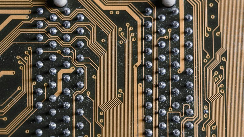
Cambridge के Department of Materials Science ने Science Advances में एक paper publish किया जो एक memristor describe करता है — एक तरह का chip component जो memory और computation को same place में combine करता है — modified hafnium oxide से built। numbers striking हैं: switching currents conventional oxide memristors से लगभग एक million गुना कम, सैकड़ों distinct stable analog conductance levels (binary on/off के बजाय), और headline claim that current digital chips के मुक़ाबले AI energy use में 70% तक reduction। mechanism brain synapses के काम करने जैसा है — discrete digital state के बजाय connection strength का gradual, analog adjustment। Lead author Dr. Babak Bakhit main barrier note करते हैं: fabrication process को अभी 700°C के आसपास temperatures चाहिए, जो standard semiconductor manufacturing lines के साथ incompatible है जो उससे कम पर top out होती हैं।
ये क्या है और क्या नहीं है। Memristors नए नहीं हैं — 1971 में theoretically describe हुए और 2008 में physically realize — पर practical, energy-efficient, manufacturable वाले दो दशकों से research frontier रहे हैं। Cambridge का contribution materials science है: filamentary switching पर depend करने के बजाय (जहाँ tiny conductive paths form और break होते हैं, जो finicky और high-energy है), उन्होंने hafnium oxide को added strontium और titanium plus two-step growth process के साथ engineer किया ताकि interfaces पर p-n junctions बनें — standard semiconductor electronics में पहले से मौजूद gates के microscopic versions की तरह। वो choice उन्हें «in-memory computing» के लिए ज़रूरी stable analog levels देता है, जहाँ same physical components data store करते हैं और math करते हैं, memory और processor के बीच back-and-forth eliminate करते हुए जो modern chip के energy budget का ज़्यादातर consume करता है। 70% figure neuromorphic computing के बारे में category claim के तौर पर meaningful है, इस specific device की specific baseline के against verified property के तौर पर कम।
ये non-specialists के लिए क्यों मायने रखता है। AI का energy footprint real public conversation बन गया है — data centers nuclear PPAs खरीद रहे हैं, town boards water और power use की वजह से compute facilities reject कर रहे हैं, frontier labs orbital data centers के बारे में openly बात कर रहे हैं क्योंकि terrestrial constraints काट रहे हैं। current architecture (separate memory और compute, data के बीच shuttling) AI को इतना power-hungry बनाती है, math खुद नहीं। In-place compute करने वाले neuromorphic chips principle में AI inference का electricity bill एक order of magnitude कम कर सकते हैं, उसी तरह जैसे brain लगभग 20 watts पर चलता है vs Llama-class model को similar reasoning के लिए kilowatts चाहिए। क्या ये specific Cambridge device वहाँ पहुँचता है या research prototype रहता है ये लगभग पूरी तरह depend करता है इस पर कि क्या कोई fabrication को standard CMOS temperatures (~450°C के नीचे) पर चलाने के लिए re-engineer कर सकता है। multiple labs lower-temperature memristor processes पर काम कर रहे हैं; Cambridge team claim नहीं कर रही कि उन्होंने वो crack किया है, बस ये कि उनके पास stable analog device है जो temperature problem solve होने पर integrate करने लायक है।
actually क्या expect करना है। Neuromorphic computing पंद्रह सालों से «पाँच साल दूर» है; ये paper उस timeline को dramatically नहीं बदलता। ये जो करता है वो उन approaches की pipeline में एक और credible architecture add करता है जो scale पर plausibly काम कर सकती हैं, Intel के Loihi, IBM के NorthPole और विभिन्न startup efforts (Rain AI, BrainChip, Synthara) के साथ। everyday users के लिए, honest expectation ये है कि अगले तीन साल में AI energy efficiency improvements algorithmic optimization (model distillation, speculative decoding, KV cache compression) और better digital silicon (Blackwell → Rubin, AMD MI400, Google TPU 8) से आएंगे neuromorphic chips के बजाय। 2028 के बाद, अगर labs Cambridge paper द्वारा highlighted manufacturing temperature constraint solve कर लें, neuromorphic accelerators research से specialized deployment में move हो सकते हैं — शायद पहले edge devices में (always-on voice, sensor analysis) जहाँ watts-saved math सबसे compelling है, और बाद में data center inference में। paper real progress है; timeline अभी भी chip-fab generations में measured है, product cycles में नहीं।