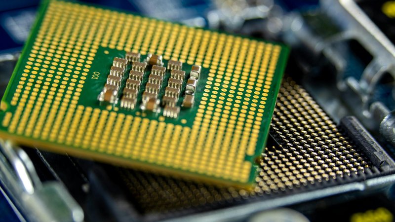
Google unveiled the 8th-generation TPU with a structural change in how the chip family is organized: TPU 8t for training, TPU 8i for inference, two distinct silicon products instead of one general-purpose part. The training chip claims 3x compute over the previous generation, with a single superpod reaching 9,600 chips and two petabytes of shared high-bandwidth memory, scaling almost linearly to a million chips in one local cluster. The inference chip targets 80% better performance per dollar, with up to 288GB of memory per chip — more than NVIDIA's Blackwell B200 at 192GB and over 3x Hopper H100's 80GB. The framing Google chose is that agents have qualitatively different demands than traditional ML inference, and a single chip optimized for both ends up compromised on each.
The architectural choices that matter for builders. The 8i inference chip is optimized for long contexts and memory-heavy operations — the workload shape modern agents have, where KV cache dominates and multi-turn state lives in working memory. Doubled interconnect bandwidth at 19.2 Tb/s targets Mixture-of-Experts models specifically, where expert routing creates all-to-all communication patterns that strangle conventional fabrics. The new Boardfly topology cuts maximum network diameter by more than 50% versus the prior generation — that's a topology-level improvement that helps both training collectives and inference parallelism. The 8t training chip's 121 ExaFlops on a single superpod means frontier model training drops from months to weeks at the per-cluster level. Two-petabyte shared HBM at the superpod scale is what enables training models with on-chip parameter residency for the largest dense backbones — the Gemini-class models being trained today wouldn't fit at scale on prior TPU generations without aggressive sharding overhead.
The ecosystem read pairs with two threads from earlier this week. Astera Labs Scorpio shipped open-standard memory-semantic fabric for non-NVIDIA training clusters; Google's 8th-gen TPU is the closed counter-direction — vertically integrated training silicon plus inference silicon plus interconnect plus topology, all designed together. The split between training and inference chips mirrors what NVIDIA hasn't fully done yet (B200 + Spectrum-X are workload-flexible by design) and what AMD is approaching with the MI300X/MI325X variants but more loosely. For builders consuming Google Cloud TPU, the practical implication is that you'll pick training tier vs inference tier explicitly going forward — the same checkpoint runs on both but at different efficiency profiles. For builders consuming GCP via inference APIs (Vertex, Gemini), the 80%-better-perf-per-dollar figure on 8i flows through to per-token pricing in some form. For builders evaluating closed-frontier vs neocloud-on-AMD, the TPU specs change the closed-frontier calculus — Google's vertical stack is now meaningfully ahead on inference memory and MoE topology, which is the workload shape where Gemini/PaLM-class agents live.
Practical move: if you run inference at scale on Google Cloud, plan a TPU 8i evaluation when it ships — 288GB memory per chip changes what you can hold in cache and what context lengths fit without paging. If you train your own models and consume TPU pods, the 8t cluster economics will be different — model your costs at the new ExaFlops/$ ratio and check whether longer-but-cheaper or shorter-but-more-expensive training pulls become more attractive. For builders not on GCP, the relevant signal is competitive pressure: NVIDIA's next-gen Rubin and AMD's MI400 ship later this year, and the inference-vs-training silicon split is going to be the architectural conversation those launches respond to. Memory per chip is the line to watch — 288GB sets a new floor for what builders should expect at inference scale by mid-2027.